00:24:21
How AMD's Next-Gen Chiplet Design in Strix Halo Hints at the Future of Zen 6
AMD is fundamentally reinventing its chiplet architecture with new silicon, advanced packaging, and a revolutionary layout. The recently discovered Strix Halo mobile APU provides a tangible preview of this future, incorporating key design elements expected in the upcoming Zen 6 architecture.
A Visual and Architectural Departure
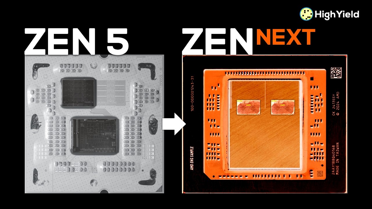
Unlike AMD's chiplet designs since Zen 2, Strix Halo presents a radically different physical appearance. Its three-die configuration—two Zen 5 CPU chiplets (CCDs) and a massive SoC die—is manufactured on TSMC's N4P node. The SoC die itself is over 2.5 times larger than the I/O die in current Ryzen 9000 desktop processors, signaling a significant shift in design philosophy.
This new layout visually resembles Intel's tile-based designs like Lunar Lake and Arrow Lake, moving away from the distinct chiplet look that has defined AMD's processors for years.
Decoding the Strix Halo SoC Die: An Unprecedented Memory and GPU System
Detailed die shots reveal the core of Strix Halo's innovation lies in its integrated graphics and memory architecture. The SoC die features a symmetrical memory subsystem with:
- Four 32-bit LPDDR5X memory PHYs on each side, creating a total 256-bit interface.
- Dedicated memory controllers adjacent to each PHY.
- A massive 32MB MALL cache (Infinity Cache), organized into eight 4MB clusters.
This dual high-bandwidth memory system exists to feed the centerpiece of the die: a discrete-class integrated GPU with 40 RDNA 3.5 compute units. This GPU power rivals dedicated graphics cards like the RX 7600 XT, enabling high-fidelity gaming on a mobile APU. The die also incorporates a 32-core XDNA NPU, media engines, and PCIe 4.0 connectivity.
The Zen 6 DNA: A Revolutionary Die-to-Die Interconnect
The most significant revelation is found at the top of the SoC die and the bottom of the CCDs: a new type of interconnect. This replaces the SerDes (Serializer/Deserializer) blocks used in all previous Zen architectures with what appears to be a vast "sea of wires."
This is the physical manifestation of a fan-out interconnect, likely utilizing TSMC's InFO_oS (Integrated Fan-Out on Substrate) packaging technology. Unlike the serial communication of the old Infinity Fabric, this new method uses an organic redistribution layer (RDL) to create hundreds of direct, parallel connections between chiplets.
The Shortcomings of the Old Infinity Fabric
To understand why this change is crucial, one must look at the limitations of the current design. The SerDes-based Infinity Fabric interconnect:
- Consumes significant power (approx. 2 picojoules per bit) for serializing/deserializing signals.
- Adds latency due to the signal transformation process.
- In consumer Ryzen CPUs, one of the two available links per CCD often goes unused ("GMI-narrow"), limiting bandwidth.
The Advantages of the New Fan-Out Interconnect
AMD's shift to a fan-out design directly addresses these weaknesses, offering major benefits:
- Dramatically Improved Power Efficiency: Eliminating the power-hungry SerDes reduces energy consumption for data transfer between chiplets by orders of magnitude, which is critical for mobile and server applications.
- Radically Reduced Latency: The interconnect acts as a direct extension of the chip's internal fabric, removing the processing delays inherent to SerDes.
- High Bandwidth: While not the primary goal, the high density of connections provides ample bandwidth. Early testing on Strix Halo shows memory write speeds exceeding 200 GB/s.
Trade-offs and Implications for 3D V-Cache
This advanced packaging does come with trade-offs. The InFO_oS technology is more complex and expensive than previous packaging methods. It also demands that chiplets be placed immediately adjacent to one another, reducing layout flexibility.
Furthermore, this new architecture poses a significant question for the future of AMD's 3D V-Cache. The complex, multi-layered RDL makes it highly challenging to integrate a cache chiplet *beneath* the CPU die, as done with the recent Zen 5 X3D processors. It is more likely that for future generations, the 3D V-Cache will return to a design where it is stacked *on top* of the CPU compute die.
Conclusion: Strix Halo as a Blueprint for the Future
Strix Halo is far more than a powerful mobile APU; it is a functional prototype for AMD's next-generation chiplet architecture. Its fan-out interconnect represents a necessary evolution, moving beyond the constraints of the SerDes-based design that served the company well since Zen 2.
This technology will be most impactful in mobile and server markets where power efficiency is paramount. For desktop users, the key benefit will be reduced latency. The discovery of this technology in a shipping product confirms that AMD's future CPUs, including those based on the Zen 6 architecture, will be built on a fundamentally more efficient and responsive interconnect foundation.
 How AMD's Next-Gen Chiplet Design in Strix Halo Hints at the Future of Zen 6
China's New Fourth-Generation Armor: A Strategic and Technical Analysis
How AMD's Next-Gen Chiplet Design in Strix Halo Hints at the Future of Zen 6
China's New Fourth-Generation Armor: A Strategic and Technical Analysis
 Beyond New Syntax: How C# 14 Is Systematically Removing Verbose Code
 David Heinemeier Hansson: Programming, Ruby on Rails, and Life Beyond Code
 Europe's Strategic Blind Spot: Why China Views the Continent as Invisible
 Why Chinese Equities Are Rallying Despite a Cooling Economy
 From Side Project to $40K/Month: How a Simple Waitlist App Outperforms Giants
 Is MVVM a Bad Architecture Choice for SwiftUI in 2025?
 Sam Altman Unveils GPT-4's Breakthroughs and AGI Roadmap
 Is China Heading Toward a "Lost Decades" Scenario? Deflation, Property Crisis, and Consumer Gloom
 Communicate with Impact: Master the Art of Smart Brevity
 Why China's Semiconductor Industry is Confidently Pushing Forward Without Nvidia Chips
 How to Win When AI Changes Everything: Key Insights from Sam Altman
 Mastering Social Media Marketing: Your Comprehensive Guide to Building Brands and Boosting Sales
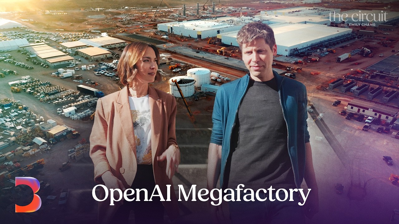
 Inside OpenAI's $500 Billion Stargate: The AI Megafactory Reshaping Tech and Society
 Building a True MVP: How to Launch Fast and Validate Your Idea
 Sam Altman Unveils GPT-5: Capabilities, Future of AI, and Societal Impact
 Testing GLM-4.5 via Claude Code: A Practical Review of Coding Performance and Alternatives
 How Luckin Coffee’s U.S. Expansion Challenges Starbucks' Dominance
