00:14:33
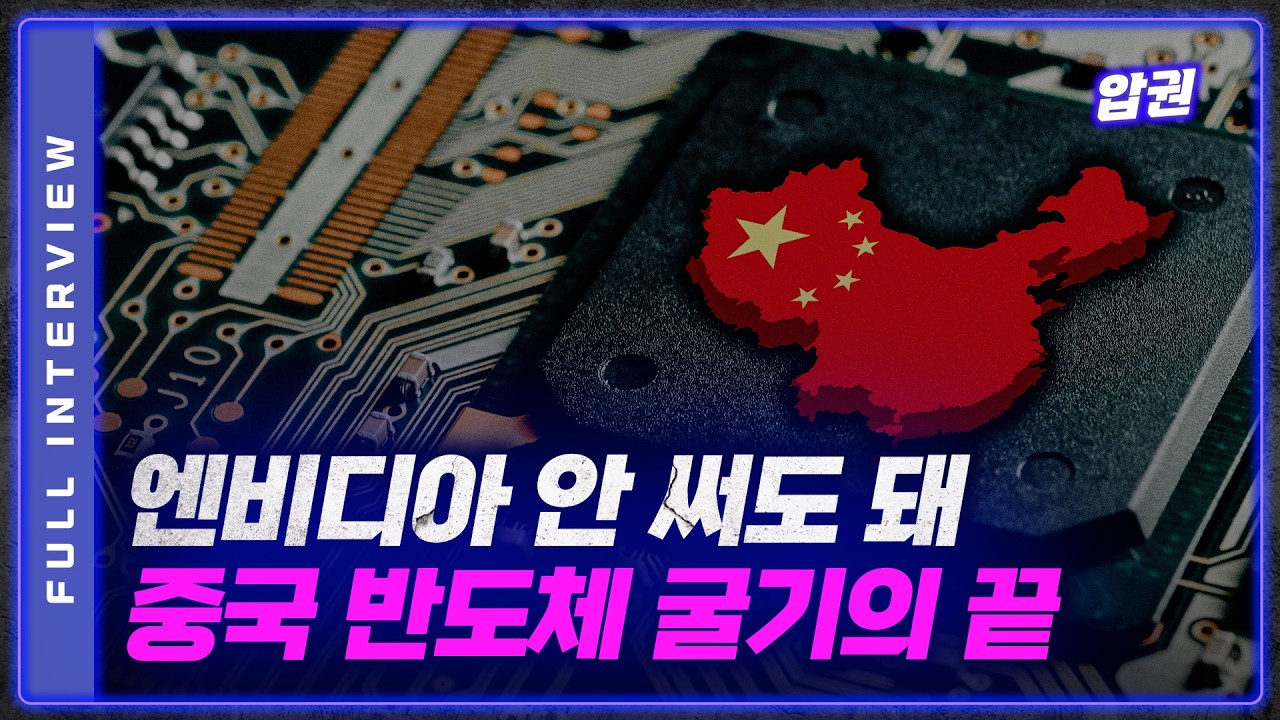
China's Two Recent Lithography Breakthroughs: Real Products, But Why Can't They Solve the EUV Dilemma?
In the ongoing US-China tech war, semiconductors remain a primary battleground. A key US strategy involves restricting China's access to advanced chips and the equipment needed to manufacture them—most critically, Extreme Ultraviolet (EUV) lithography machines from Dutch company ASML. Despite China's desire, it has been unable to purchase a single EUV system. However, this month, two separate Chinese institutions announced successful developments of similar, alternative technologies. This article breaks down what these new products are, how they differ from ASML's EUV, and explores the puzzling reality: why genuine technological breakthroughs might not be enough to break the American-led export restrictions.
Breakthrough 1: Nanoimprint Lithography (NIL) from Prinano
On August 8th, Hangzhou-based Prinano (璞璘科技) announced the successful delivery and acceptance of its first PL-SR series step-and-repeat nanoimprint lithography (NIL) equipment to a domestic customer on August 1st. The customer, described as focusing on "specialty processes," opted to remain anonymous, likely to avoid attracting undue attention.
What is Nanoimprint Lithography (NIL)?
NIL is not a new technology; its foundations were laid in the 1990s. A seminal 1996 paper by Professor Stephen Y. Chou (周郁) from Princeton University introduced the term "nanoimprint lithography," proposing a method to create nanoscale circuit patterns—a staggering concept at a time when industry standards were still measured in microns.
Unlike traditional photolithography, which uses light (e.g., 193nm DUV or 13.5nm EUV light) to project a circuit pattern onto a photoresist-coated wafer, NIL uses a physical quartz template (or mold). This template, itself fabricated using electron-beam lithography, is pressed into a softer layer on the wafer called the imprint resist. The pattern is then solidified through processes like heating or UV curing.
The Commercial Milestone and Inherent Challenges
The technology's commercial potential was only recently demonstrated by Japan's Canon, which launched its first commercial NIL semiconductor production equipment, the FPA1200 NZ2C, in October 2023. Canon's system boasts advantages: it consumes about 90% less power than an EUV machine and costs less than half the price, supporting linewidths down to 14nm (equivalent to the industry's "5nm node").
However, NIL faces significant hurdles for widespread adoption, especially in complex logic chips:
- Low Throughput: The process is slow. While ASML's latest EUV tools can process over 175 wafers per hour, NIL equipment struggles to reach 100 wafers per hour.
- Alignment Accuracy: Precisely aligning multiple layers (a chip can have over 100 layers) is a critical weakness of NIL. Prinano's own specs note an alignment accuracy of less than 200nm, which is insufficient for advanced multi-layer patterning despite achieving sub-10nm linewidths.
- Template Wear and Contamination: The physical process of stamping and demolding can lead to template degradation and introduce contaminants (defects), impacting yield.
- High Process Conversion Cost: Integrating NIL requires a complete overhaul of existing fabrication processes, which is prohibitively expensive for most foundries.
Therefore, while Prinano's achievement in delivering a sub-20nm tool is notable, its current limitations prevent it from being a viable substitute for EUV in manufacturing cutting-edge logic chips. Its most promising application lies in memory chips like NAND Flash, where circuit patterns are simpler and repetitive.
Breakthrough 2: Electron-Beam Lithography from Yuhang Quantum Institute
On August 14th, the Yuhang Quantum Institute (餘杭量子研究院), associated with Zhejiang University, announced that China's first home-grown commercial electron-beam lithography (EBL) system, named "Xī Zhī" (羲之), had begun application testing.
What is Electron-Beam Lithography?
EBL is an even older technology, pioneered in the 1960s by Bell Labs and UC Berkeley. It operates on a fundamentally different principle: a focused beam of electrons directly "writes" a circuit pattern onto an electron-sensitive resist, point by point. This method achieves exceptionally high resolution, capable of defining features well below 10nm.
The Fundamental Limitation: Throughput
The primary and insurmountable drawback of EBL for mass production is its extremely low throughput. Writing a pattern with a single electron beam is an incredibly slow process:
- A single-beam system could take up to a month to pattern a single 12-inch wafer.
- Even advanced multi-beam systems might still require over an hour per wafer.
This stands in stark contrast to the hundreds of wafers per hour processed by DUV and EUV lithography systems. Consequently, EBL has never been and will never be used for high-volume chip manufacturing. Its critical applications are in research & development and the fabrication of the masks (photomasks) and NIL templates used by other lithography tools.
Labeling the "Xī Zhī" as a "lithography machine" creates a misleading comparison to ASML's mass production tools. It is a specialized tool for specific, low-volume tasks, not a solution for producing chips at scale.
Conclusion: Real Progress, But Not a Game Changer
The development of both NIL and domestic EBL systems represents authentic technological progress for China's semiconductor equipment industry. However, these breakthroughs do not equate to a solution for China's inability to acquire EUV technology.
Nanoimprint Lithography remains a complementary technology, potentially suitable for specific memory chips but hampered by throughput and alignment issues that make it uncompetitive with EUV for leading-edge logic chip production in the foreseeable future.
Electron-Beam Lithography is fundamentally incapable of mass production due to its abysmal throughput, confining its role to R&D and mask-making.
These developments are significant as markers of China's determined, incremental progress in navigating US semiconductor restrictions. Yet, they fall short of altering the fundamental dynamics of the tech war. True commercial viability and the ability to challenge the established ecosystem led by companies like ASML will depend on achieving not just technological capability, but also high yield, high throughput, and cost-effective mass production—a challenge that continues to elude many established players, let alone newcomers.

