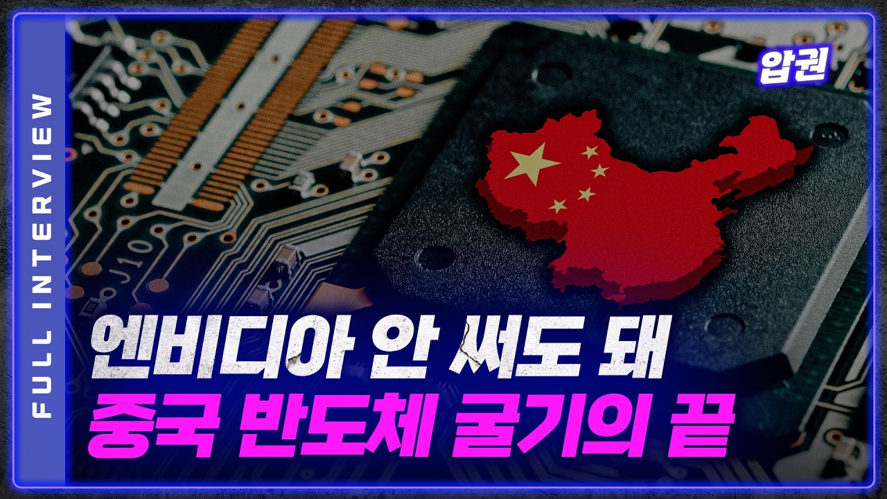
01:01:43
The New Cold War: Why Semiconductors Will Define U.S.-China Tech Dominance
As geopolitical tensions escalate around advanced semiconductor technology, this in-depth analysis examines:
• Core chipmaking technologies targeted by export controls
• Breakthroughs prolonging Moore's Law
• Why only ASML's EUV machines can build leading-edge chips
• China's push for semiconductor self-reliance amidst restrictions
Electronic Design Automation: The Blueprint Barrier
Semiconductors underpin modern technology, from smartphones to military systems, containing billions of microscopic transistors. With the U.S. restricting sub-3nm chip design tools to China, Electronic Design Automation (EDA) has become a critical geopolitical battleground. These sophisticated software suites manage the immense complexity of modern circuit design by:
- Providing pre-validated IP blocks and circuit libraries
- Running billions of simulations to verify functionality
- Optimizing chip layouts across hundreds of parameters
American firms Synopsys, Cadence and Siemens EDA dominate nearly 80% of this $14B market, benefiting from decades of development and partnerships with major foundries. Chinese alternatives like Empyream and Cellix remain constrained to older 28nm+ process technologies. Crucially, EDA development requires close collaboration with cutting-edge fabs – a severe limitation for China after the U.S. excluded Samsung from expanding advanced nodes in China via the 'Chip 4' framework.
Transistor Innovations: Scaling Beyond Moore's Law
| Structure | Development Era | Fundamental Limitation |
|---|---|---|
| Planar FET | Pre-2011 | Gate control degradation at 20nm+ |
| FinFET | 20nm to 3nm nodes | Insufficient surface contact at <3nm |
| GAAFET | Post-3nm | Requires revolutionary new EDA tools |
Current U.S. export controls explicitly target GAAFET development – a "gate-all-around" structure essential to achieving true 3nm and 2nm designs. This technology involves vertically stacked silicon nanowires, allowing transistors to circumvent the leakage current issues that plague shrinking FinFET designs, extending transistor density scaling beyond current physical limits.
EUV Lithography: ASML's Global Monopoly
Lithography machines blueprint circuits onto silicon wafers using extreme ultraviolet light (EUV). Dutch manufacturer ASML dominates this field because their $200M machines overcome fundamental physical limitations:
- 13.5nm wavelength enables sub-10nm features (vs 193nm in previous DUV systems)
- Reflective mirrors replace standard lenses destroyed by EUV energy
- Positioning accuracy below 50 picometers (smaller than hydrogen atoms)
After years of R&D failure with U.S. and Asian competitors, ASML emerged as the only supplier qualified for modern foundries. This critical bottleneck impacts every component vendor: high-purity silicon wafers from Japan (88% 11N grade market share), lens modules from Germany, and specialized chemicals from Ohio suppliers. With 2023 Dutch cooperation on U.S. embargoes, China's champion foundry SMIC cannot obtain replacement units, forcing reliance on costly multipatterning and advanced DUV – yielding inferior performance at non-competitive operational scales.
Advanced Packaging Technologies: Escaping 2D Scaling
When transistor shrinkage stalled, manufacturers turned vertically. TSMC's 3DFabric Alliance consolidates innovations like SoIC and CoWoS to embed logic chips atop memory units via:
- Through-silicon-vias (TSVs): Vertical interconnects bypassing bonding wires
- Ultra-precision placement: ±0.1μm chip-to-wafer stacking (using IR detection)
- Heterogeneous structures: Combined DDR5+AI accelerators enabling quantum leaps
The resulting system-in-package architecture within Apple's M-series cuts power consumption 34% while quadrupling bandwidth – achievements traditional EScaling cannot match. Nevertheless, cooling 700W/m² heatflux within microjunctions remains an engineering challenge needing novel adhesives and thermal interfaces beyond mainstream assembly lines.
Frontier Manufacturing Chemistry: Sub-Nanometer Fabrication
To deposit insulator gates below atoms thick, foundries rely on revolutionary Atomic Layer Deposition (ALD). This cyclic vapor application builds materials sequentially through self-limiting monolayer reactions – drastically reducing edge nonuniformity seen in CVD methods. Key innovations:
Plasma-enhanced ALD: Reactive ion bombardment allowing low-temp processing crucial for advanced materials like ruthenium electrode substrates while avoiding component degradation.
Hybrid applications: Integrating ALD dielectric stacks between epitaxial layers for reliable FinFET conduction without leakage channels.
Over 85% market share in sub 5nm transistor films belong to equipment leader ASM through advanced surface engineering expertise and co-optimization with exposure patterning ecosystems.
AI Acceleration Ecosystems: Beyond Traditional Silicon
Customized Tensor Processing Units (TPUs) represent computation's next evolution by using "systolic array" architecture. Contrasted against conventional processors:
Generic x86 Computing
- • Decentralized instruction scheduling latency
- • Inefficient matrix multiplications
- • Cache hierarchy bottlenecks at TB-scale transfers
Tensor Optimizations
- • Dataflow directly between neighbor cores
- • Native 128x128 grid operations
- • Unified L1 shared memory pool at compute units
This allows Google's latest smartphone chips like Tensor G2 to accomplish real-time object removal and adaptive Super Res Zoom using dedicated neural calculations – tasks impossible for traditional benchmarks scoring equally. Even mundane functions like transcribing Mandarin or filtering background noise occur with 90% computational efficiency.
Strategic Crossroads for Global Technology
The semiconductor value chain is both fragile and interdependent. Maintaining innovation leadership requires multi-trillion dollar infrastructure covering photoresist manufacturers in Kumamoto prefecture, gas production in South Korean complexes, quartz crystal fabrication in Portland facilities, alongside software expertise concentrated primarily in Western technology centers.
Current international control enforcements have created two competing ecosystems:
- Global innovation framework integrating Dutch EUV hardware + U.S. EDA capabilities + Taiwanese/Japanese materials
- Parallel supply chains where China attempts internal replacement solutions while suffering ~4-generation node deficits despite significant RDFund allocation growth
Fundamental obstacles remain: Developing viable indigenous EUV alternatives require breakthroughs past plasma confinement barriers around 100W at 13.5nm bandwidth – a problem unsolved after $20B cumulative Western research investment.


